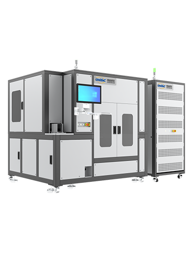
The system is capable of chip testing, including Vth testing, gate leakage current testing, drain leakage current testing, and GB/RB testing
Supports customizable experimental programs and failure determination
Equipped with automatic visual alignment and wafer ID recognition
Supports wafer MAP input and recognition
Long-term high-temperature operating capability
Applicable Wafer: Automotive SiC MOSFET wafer, compatible with 4, 6, 8 Inch
Burn-in Test: HTGB, HTRB
Temperature: RT - 200℃
Voltage Range: HTGB: up to ±75V; HTRB: up to 2000V
Test Layer:Manual version: 1;Automatic version: up to 6 layers (3+3)
Test Channels per Wafer: Up to 1300
Test Range: HTGB: IGSS (±10nA~±1A);HTRB: IDSS (100nA~20mA);Before & after burn-in: VGS(th) (20mV~200V)
Test Accuracy: VGS(th) : 0.015% + 1mV (@20V), IGSS: 0.060% + 100pA (@100nA), IDSS: 0.1% (@1μA)
Avoid Arcing:Sealed design, supports 0.6MPa CDA or N2
Burn-in Probe Card:Supporting Customization According to Wafer,electrical performance, structural performance to meet the test requirements